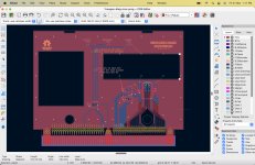
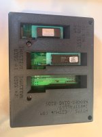
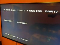
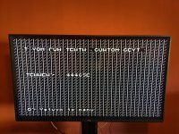
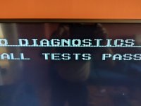
I've been wanting to do this for a long while. One of the deficiencies of the neogeo diag bios is the inability to help when a motherboard boots to crosshatch. I decided to take a stab at creating a custom prog board to help with this situation. With it, its possible to verify P rom output, address/data lines, and p2 region is writable (carts use this for bank switching).
I started with a proof of concept using breadboard with 2 extra 64K sram chips I had. I wired them up to a P rom socket along with a couple 74 series logic chips to handle enable/write logic.
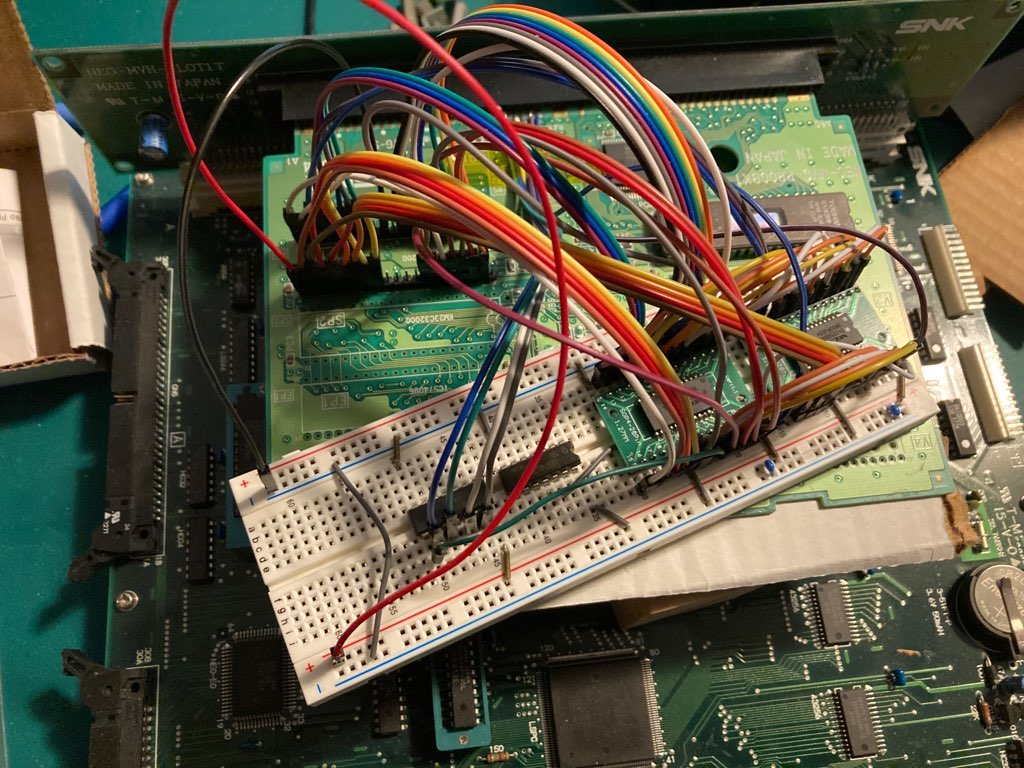
I wrote up some test code to verify it was working as I was expected and it seemed to be. But 2x64K is only 1Mbit of the 8Mbit address space I would need for full testing. I found some 8Mbit 16-bit 5V srams on digikey and got one wired up.
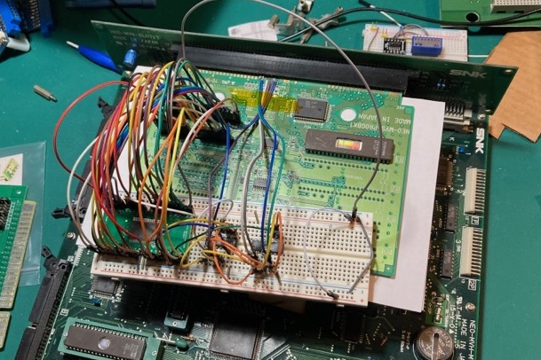
This worked well too. This breadboard setup made it easy to simulate errors to very the new code in the diag bios was detecting the errors.
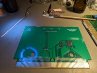
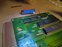
Next step was to get all this on a pcb. This was the initial version
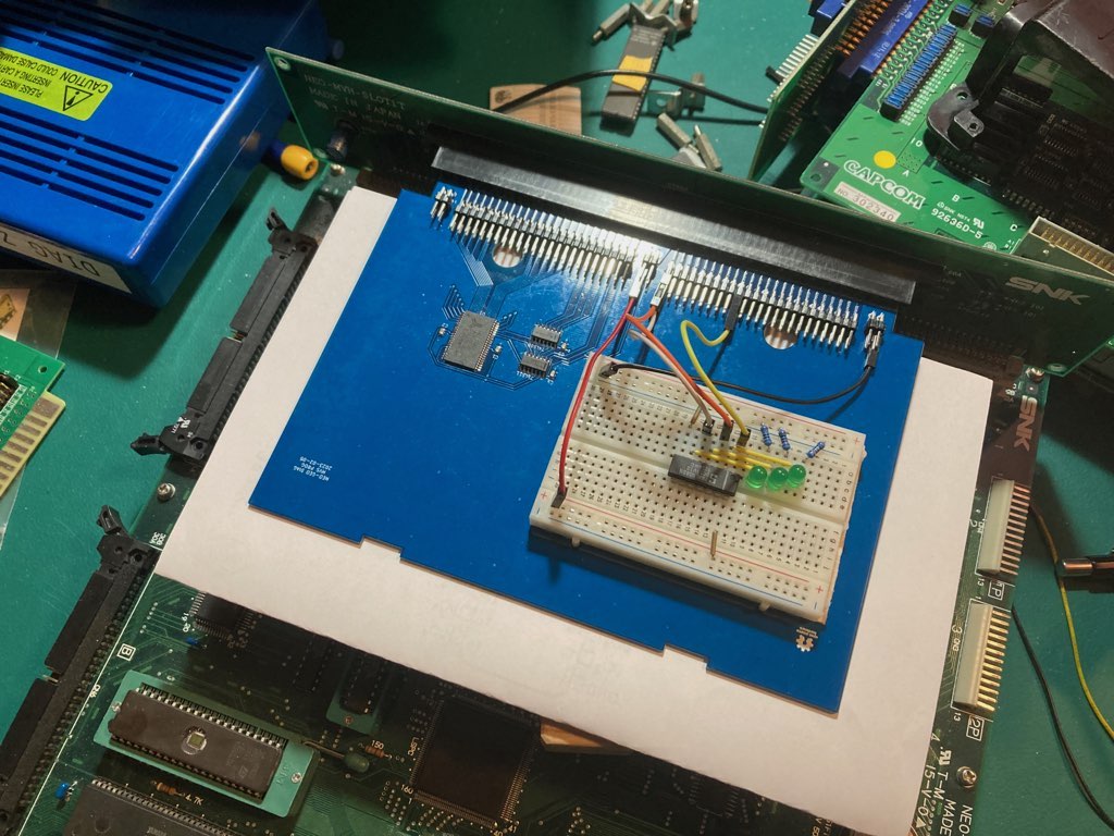
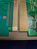
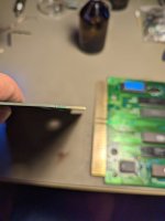
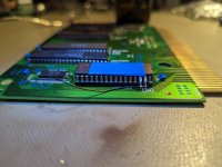
Thankfully it worked. The only issue was a little bit of side to side play when the board was in the slot, which I fixed in the next revision.
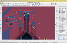
Its hard to tell from the picture but there are through holes for each signal (and signal labels) to make it easier to debug crosshatch/slot issues.
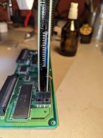
In the above picture I ended up soldering in some right angle connectors in the through hole to make it easier to test some stuff related to the board design. The breadboard is me wiring up a couple signals related to the P rom to LEDs because they aren't something you can test for from the CPU. This will let you verify the signals are becoming active during the test loop.
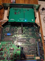
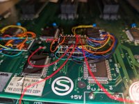
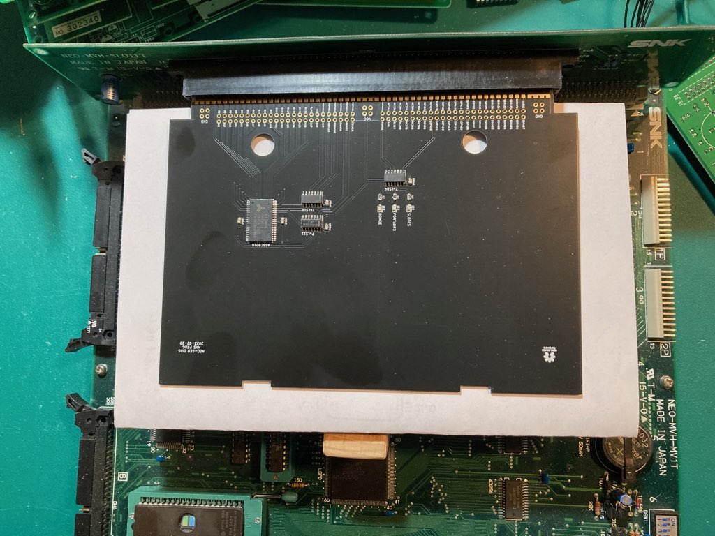
This is the latest revision and where things are currently.
There are still a few things to do
I started with a proof of concept using breadboard with 2 extra 64K sram chips I had. I wired them up to a P rom socket along with a couple 74 series logic chips to handle enable/write logic.
I wrote up some test code to verify it was working as I was expected and it seemed to be. But 2x64K is only 1Mbit of the 8Mbit address space I would need for full testing. I found some 8Mbit 16-bit 5V srams on digikey and got one wired up.
This worked well too. This breadboard setup made it easy to simulate errors to very the new code in the diag bios was detecting the errors.
Next step was to get all this on a pcb. This was the initial version
Thankfully it worked. The only issue was a little bit of side to side play when the board was in the slot, which I fixed in the next revision.
Its hard to tell from the picture but there are through holes for each signal (and signal labels) to make it easier to debug crosshatch/slot issues.
In the above picture I ended up soldering in some right angle connectors in the through hole to make it easier to test some stuff related to the board design. The breadboard is me wiring up a couple signals related to the P rom to LEDs because they aren't something you can test for from the CPU. This will let you verify the signals are becoming active during the test loop.
This is the latest revision and where things are currently.
There are still a few things to do
- A couple minor tweaks to this MVS version
- Finish up the AES version (95% done)
- Write up docs on the different tests
- Go over diag bios changes again


